Nano SIM Card Connector SMT Mounting: PCB Footprint Design, Soldering Guidelines, and Process Considerations
Introduction: Why SMT Mounting Matters for Nano SIM Card Connectors
Surface Mount Technology (SMT) has become the standard assembly method for Nano SIM Card Connectors in modern electronic devices. As IoT modules, wearable technology, 5G terminals, and industrial communication equipment continue to shrink in size while demanding higher reliability, proper SMT mounting of Nano SIM connectors is critical to achieving consistent electrical performance, mechanical stability, and long-term durability in production volumes.
Unlike through-hole (DIP) connectors, SMT Nano SIM connectors are soldered directly onto the PCB surface without drilled holes. This approach enables thinner device profiles, higher assembly throughput, and lower manufacturing costs. However, it also introduces specific design and process challenges that engineers must address during PCB layout, solder paste application, reflow profiling, and quality inspection.
This guide provides a comprehensive engineering overview of Nano SIM card connector SMT mounting — covering PCB footprint design, stencil and solder paste considerations, reflow soldering profiles, common defects and their root causes, and inspection criteria to ensure reliable production outcomes.

Understanding Nano SIM Connector Package Types for SMT
Nano SIM card connectors (4FF form factor) are available in several package configurations, each suited to different design requirements and assembly processes. The choice of connector package directly influences PCB footprint design, solder joint geometry, and reflow process parameters.
Top-Mount SMT Connectors
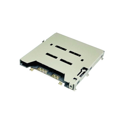
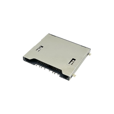
Top-mount connectors are the most common type for Nano SIM applications. The connector body sits on top of the PCB, and all solder terminals are located on the same side as the component body. These connectors offer straightforward assembly, easy visual inspection, and compatibility with standard reflow processes. MOARCONN’s 1.10mm height Push-Pull Nano SIM connector is a typical top-mount SMT design with 1.20mm pitch and 6-pin configuration.
Bottom-Mount SMT Connectors
Bottom-mount connectors position the solder terminals on the underside of the connector body, allowing the component to sit lower on the PCB. This design saves additional vertical space but may require special consideration for solder paste deposition and inspection, as the solder joints are partially hidden beneath the component.
SMT vs. DIP: When to Choose Each
| Parameter | SMT Connector | DIP Connector |
|---|---|---|
| Profile Height | Lower (1.10–1.44mm typical) | Higher (requires through-hole clearance) |
| Assembly Throughput | Higher (reflow batch processing) | Lower (wave soldering or hand soldering) |
| Solder Joint Reliability | Shear stress on solder pads | Stronger mechanical anchor through holes |
| Inspection Accessibility | Easy visual and AOI access | Requires X-ray for hidden joints |
| Rework Complexity | Hot-air rework with nozzle | Desoldering required, higher board stress |
Key Note: For most IoT modules, wearable devices, and portable electronics, SMT Nano SIM connectors offer the best balance of space utilization, assembly efficiency, and cost. DIP connectors remain suitable for applications requiring very high mechanical retention under continuous vibration, such as automotive telematic control units.
PCB Footprint Design for Nano SIM Connectors
The PCB footprint is the foundation of a reliable SMT solder joint. A poorly designed footprint can lead to tombstoning, insufficient solder fillet, or poor alignment during reflow. Engineers should follow these guidelines when designing the PCB land pattern for a Nano SIM card connector.
Pad Geometry and Dimensions
Each solder pad on the PCB should extend approximately 0.2–0.5mm beyond the connector terminal footprint to allow adequate solder fillet formation. The pad width should match or slightly exceed the terminal width, typically 0.30–0.50mm for 1.20mm pitch Nano SIM connectors. Pad length should accommodate both the terminal contact area and the solder fillet, usually 1.0–1.5mm total.
Keep-Out Zones and Clearance
Nano SIM connectors require unobstructed keep-out areas around the card insertion and ejection path. No components, vias, or tall solder joints should be placed within 1.0–1.5mm of the card slot opening. The connector body also requires clearance from nearby tall components to facilitate pick-and-place nozzle access during assembly. For push-pull type connectors, ensure at least 2.0mm clearance on the insertion side for card access by the end user.
Thermal Management on the PCB
Uneven thermal mass across the connector’s solder pads can cause tombstoning or skewed placement during reflow. Design the PCB such that all pads under the connector have similar copper trace widths and thermal relief connections. Avoid connecting one pad directly to a large copper pour while others connect through narrow traces — this creates thermal imbalance that leads to inconsistent solder melting and solidification.
Solder Mask and Pad Finish
Solder mask-defined (SMD) pads are recommended for fine-pitch connectors to prevent solder bridging between adjacent terminals. For Nano SIM connectors with 1.20mm pitch, a solder mask web of 0.20–0.30mm between pads provides adequate insulation. Recommended PCB pad finishes include ENIG (Electroless Nickel Immersion Gold) and HASL (Hot Air Solder Leveling), with ENIG preferred for fine-pitch applications due to its flat surface and excellent solderability.
Solder Paste and Stencil Design
The solder paste deposition process determines the volume and geometry of solder available for joint formation. For Nano SIM connectors, stencil design parameters must be carefully selected to achieve consistent solder paste transfer and reflow results.
Stencil Thickness
A stencil thickness of 0.100–0.125mm (4–5 mil) is generally suitable for Nano SIM connector pads. Thinner stencils (0.075mm) may be used for ultra-fine-pitch designs adjacent to the connector, while thicker stencils (0.150mm) increase solder volume at the risk of bridging on closely spaced pads.
Aperture Design
Aperture dimensions should match the PCB pad dimensions or be slightly reduced (90–95% of pad area) to prevent excessive solder extrusion beyond the pad edges. For 1.20mm pitch, rectangular apertures with rounded corners improve paste release from the stencil walls. An aspect ratio (aperture width / stencil thickness) of at least 1.5 is recommended for consistent paste transfer.
Engineering Tip: For connectors with mixed terminal sizes (e.g., larger grounding terminals alongside smaller signal terminals), consider stepped stencils or localized aperture area adjustments to achieve uniform solder volume across all joints. This reduces the risk of insufficient solder on small pads or bridging on large pads.
Reflow Soldering Profile for Nano SIM Connectors
The reflow profile must be optimized for the Nano SIM connector’s solder terminals, the PCB finish, and the solder paste alloy. A typical lead-free reflow profile (SAC305 alloy) for Nano SIM connectors follows these parameters:

| Profile Stage | Temperature Range | Duration | Purpose |
|---|---|---|---|
| Preheat | 150–200°C | 60–90 seconds | Activate flux, equalize board temperature |
| Soak | 200–217°C | 60–90 seconds | Remove solvents, prepare paste for reflow |
| Reflow (Peak) | 235–250°C | 30–60 seconds above 217°C | Melt solder, form metallurgical joint |
| Cooling | ↓ to below 100°C | 2–4°C/sec ramp-down | Solidify joint, prevent thermal shock |
The peak temperature should not exceed 260°C to avoid damaging the connector’s plastic housing or degrading contact spring performance. Ramp-up rates should be controlled to 1–3°C/sec to prevent thermal shock to the connector body. Rapid cooling (above 4°C/sec) may cause excessive thermal stress on the solder joints, leading to microcracks over thermal cycling.
Common SMT Defects and Troubleshooting
Even with careful design, SMT assembly of Nano SIM connectors can encounter several common defects. Understanding their root causes helps engineers implement corrective actions quickly during production ramp-up.
Tombstoning (Drawbridge Effect)
Tombstoning occurs when one end of the connector lifts off the PCB during reflow due to uneven surface tension on opposing solder pads. This is typically caused by thermal imbalance — one pad reaching solder melting temperature before the other. Solutions include equalizing trace widths to all pads, reducing the temperature gradient across the connector, and ensuring both pad rows have similar thermal relief connections.
Solder Bridging
Bridging between adjacent pins is most common on fine-pitch connectors. For 1.20mm pitch Nano SIM connectors, bridging can result from excessive solder paste volume, insufficient solder mask web between pads, or misaligned stencil apertures. Reducing stencil thickness, increasing solder mask web width, and verifying stencil-to-board alignment during printing can mitigate this defect.
Insufficient Solder or Poor Wetting
Insufficient solder fillet on connector terminals reduces mechanical strength and may cause intermittent electrical contact. This is often caused by oxidized PCB pad finish, expired or improperly stored solder paste, or inadequate reflow temperature at the connector location. ENIG pad finish with proper storage (≤30°C, ≤60% RH) and fresh solder paste (refrigerated, within 72 hours of opening) significantly reduce wetting issues.
Connector Misalignment
If the connector shifts during reflow due to paste slump or conveyor vibration, the solder joints may be misaligned or the card slot may be offset. Ensuring sufficient solder paste tackiness, minimizing conveyor vibration, and verifying pick-and-place accuracy (±0.05mm recommended) prevent this issue.
Inspection and Quality Control
After reflow, every Nano SIM connector should undergo inspection to verify solder joint integrity and connector alignment. The following inspection methods are recommended:
Automated Optical Inspection (AOI)
AOI systems can detect solder joint defects — bridging, insufficient solder, missing components, and misalignment — by comparing the actual solder joint appearance against a trained golden-board reference. AOI is the primary inspection method for SMT lines and should cover 100% of connectors on each board.
X-Ray Inspection
For connectors with hidden solder joints or for high-reliability applications (automotive, medical), X-ray inspection provides visibility into solder voiding, head-in-pillow defects, and internal joint quality. IPC-A-610 Class 2 or Class 3 acceptance criteria should be applied based on the product’s reliability requirements.
Pull and Shear Testing
Destructive pull testing on sample connectors provides quantitative data on solder joint strength. A minimum pull force of 10N per terminal is typically required for Nano SIM connectors soldered to standard PCB finishes. Shear testing evaluates the lateral strength of the solder joint and is particularly relevant for connectors that experience card insertion forces during product use.
Design for Manufacturing (DFM) Recommendations
Integrating DFM principles early in the design phase reduces assembly defects and improves yield rates. For Nano SIM card connector SMT mounting, consider these recommendations:
- Provide at least two fiducial marks on the PCB near the connector location for pick-and-place alignment reference.
- Avoid placing microvias or through-holes within the solder pad area of the connector — this can wick solder away from the joint during reflow.
- Design symmetrical pad geometry for all terminals to reduce tombstoning risk during reflow.
- Include test points on the PCB layout for continuity testing after assembly, preferably on the SIM signal lines (VCC, RST, CLK, GND, I/O, and card detect).
- Communicate the connector manufacturer’s recommended reflow profile to the contract manufacturer during the new product introduction (NPI) phase.
- Request a first-article inspection report for the first production batch, including AOI, X-ray (if applicable), and pull test data.
Frequently Asked Questions
What is the standard reflow peak temperature for Nano SIM connectors?
The peak reflow temperature should be between 235°C and 250°C for lead-free SAC305 solder, with an absolute maximum of 260°C to prevent damage to the connector’s plastic housing. The exact profile depends on the connector manufacturer’s specification and should be verified during the NPI phase.
Can Nano SIM connectors be hand-soldered?
Hand soldering of SMT Nano SIM connectors is possible but not recommended for production volumes. Fine-pitch terminals (1.20mm) require careful soldering iron control and magnification to avoid bridging. Hot-air rework stations with dedicated nozzles are preferred for prototype or rework applications.
How do I prevent solder bridging on 1.20mm pitch Nano SIM connectors?
Use a solder mask web of at least 0.20mm between adjacent pads, maintain stencil thickness at 0.100–0.125mm, and verify stencil-to-board alignment within ±0.05mm. Reduce solder paste volume by 5–10% if bridging persists.
What pad finish is best for Nano SIM connector SMT mounting?
ENIG (Electroless Nickel Immersion Gold) is the preferred pad finish for fine-pitch SMT connectors due to its flat surface, excellent solderability, and resistance to oxidation. HASL is a cost-effective alternative but may produce uneven surfaces that cause alignment issues on fine-pitch components.
How do I test the solder joint quality after reflow?
AOI is the primary inspection method for visible joints. For hidden joints or high-reliability applications, X-ray inspection is recommended. Destructive pull testing on sample units (per JEDEC or IPC standards) provides quantitative joint strength data. Continuity testing through the SIM signal lines should be performed on 100% of assembled units.
What is the recommended pull force for a Nano SIM connector terminal?
A minimum pull force of 10N per terminal is generally acceptable for standard applications. For high-reliability or automotive applications, a minimum of 15N per terminal is recommended. These values should be verified against the connector manufacturer’s specification and the end-product reliability requirements.
Summary
Successful SMT mounting of Nano SIM card connectors requires careful attention to PCB footprint design, stencil and solder paste parameters, reflow profiling, and quality inspection. By following the engineering guidelines outlined in this article — including pad geometry optimization, thermal balancing, proper stencil selection, and systematic defect troubleshooting — design and manufacturing engineers can achieve high assembly yields and reliable solder joints for mass production.
For engineers seeking reliable Nano SIM connector solutions with documented SMT specifications, MOARCONN provides a range of Nano SIM Card Connectors with validated SMT design recommendations. For detailed footprint drawings, reflow profile data, and mechanical specifications, refer to the product data sheet and 2D drawing resources.