SIM Card Connector PCB Layout: Design Rules, Keep-Out Zones, and Routing Guidelines
Introduction: Why SIM Card Connector PCB Layout Matters
The SIM card connector is a critical electromechanical component in any cellular-enabled device. While engineers often focus on selecting the right connector model and verifying its electrical specifications, the PCB layout surrounding the connector is equally important. A poorly designed SIM connector layout can cause signal integrity issues, intermittent SIM detection, ESD damage, and even field failures that are difficult to diagnose.
This guide covers the essential PCB layout rules for SIM card connectors — including recommended keep-out zones, trace routing guidelines, pad footprint design, grounding strategies, and ESD protection — to help hardware engineers design reliable cellular interfaces for IoT, industrial, and consumer devices.
1. SIM Card Connector Footprint and Pad Design
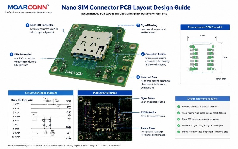
The foundation of a good SIM connector layout starts with the correct footprint. Always follow the manufacturer's recommended land pattern from the official datasheet. Key considerations include:
- Pad dimensions: Use the exact pad size specified — oversized pads can cause solder bridging, while undersized pads weaken mechanical strength.
- Solder paste stencil: For SMT connectors, use a stencil thickness of 0.12–0.15 mm with an opening ratio of 80–100% of the pad area.
- Edge clearance: Maintain at least 0.5 mm clearance from the connector body to the PCB edge for pick-and-place assembly.
- Mechanical support: For push-push connectors, consider adding additional solder pads on the metal shell for mechanical reinforcement.

2. Keep-Out Zones for SIM Card Connectors
Keep-out zones are areas on the PCB that must remain free of copper traces, vias, and components to ensure proper connector operation and avoid interference. For SIM card connectors, the following keep-out rules apply:
| Zone | Description | Recommended Clearance |
|---|---|---|
| Card insertion path | Area where the SIM card slides into the connector — no components or tall solder joints allowed | Full card travel length + 2 mm |
| Ejector mechanism | Area around the push-push or push-pull mechanism — mechanical parts require clearance | At least 1 mm on each side |
| Contact finger area | Under the connector body where contact pins touch the SIM card — no traces or vias | Full connector body footprint + 0.3 mm per side |
| Shell ground pads | Grounding pads on the connector shell for EMI and mechanical stability | At least 0.2 mm clearance to other nets |
Pay special attention to the underside of the connector. Some connectors have contact springs that protrude below the PCB mounting plane. Ensure no traces or vias are placed in these areas.
3. SIM Signal Trace Routing Guidelines
The SIM interface operates at clock frequencies typically ranging from 1 MHz to 5 MHz. While this is not a high-speed interface by modern standards, proper signal integrity practices still apply:
3.1 Trace Width and Spacing
- Route SIM traces with a minimum width of 0.25 mm (10 mil) to keep resistance low.
- Maintain at least 0.2 mm (8 mil) clearance between SIM signal traces and other nets.
- Keep all SIM traces as short as possible — ideally under 50 mm from connector to module.
3.2 Length Matching
While SIM interfaces are generally tolerant of trace length mismatches, it is good practice to keep the CLK, RST, and I/O traces roughly equal in length. Aim for a maximum skew of 10 mm between these critical signals.
3.3 Avoid Right-Angle Bends
Use 45-degree chamfered corners or arc routing instead of 90-degree bends to minimize signal reflections. This is especially important for the CLK signal.
4. Grounding and Power Delivery
A proper grounding strategy is essential for reliable SIM card operation:
- Ground plane: Provide a solid ground plane on the layer directly below the SIM connector. Avoid splitting the ground plane under the connector area.
- Multiple ground vias: Connect the connector's ground pads to the ground plane with at least 2–3 vias per pad to minimize ground inductance.
- VCC filtering: Place a 100 nF ceramic capacitor as close as possible to the SIM VCC pin (C1), ideally within 3 mm. Add a 10 µF bulk capacitor nearby if the module power supply is shared.
- Ferrite bead: For noisy environments, consider adding a ferrite bead (100 Ω at 100 MHz recommended) in series with the SIM VCC trace.
5. ESD Protection for SIM Interfaces
SIM card connectors are frequently accessed by users, making them vulnerable to electrostatic discharge (ESD). Proper ESD protection is critical:
- TVS diodes: Place low-capacitance TVS diodes (< 5 pF) on all SIM signal lines (C1–C8) within 5 mm of the connector pins.
- Series resistors: Add 10–22 Ω series resistors on the CLK, RST, and I/O traces near the connector to limit transient current.
- Discharge path: Ensure the connector's metal shell has a low-impedance path to chassis ground or PCB ground through multiple vias.
- Air gap: Maintain at least a 1 mm air gap between the SIM card slot opening and any exposed copper on the PCB edge.
6. PCB Layer Stack-Up Recommendations
For optimal SIM connector performance, use the following minimum layer stack-up:
| Layer | Function | Notes |
|---|---|---|
| Top | SIM connector and components | All SIM components on one side |
| Inner 1 | Ground plane | Uninterrupted under SIM area |
| Inner 2 | Power / signal routing | SIM VCC and other power traces |
| Bottom | Additional routing / ground | Keep clear under connector if bottom-mounted |
For 2-layer boards, ensure the bottom layer has a solid ground pour under the SIM connector area, and use stitching vias around the connector perimeter.
7. Common PCB Layout Mistakes
Based on field experience, here are the most common SIM connector PCB layout errors:
Mistake 1: Traces Under the Connector Body
Running traces directly under the SIM connector is a frequent error. The connector's contact springs can short against exposed traces during insertion, causing permanent damage.
Mistake 2: Insufficient Keep-Out for Card Insertion
Placing tall components (capacitors, inductors) in the SIM card insertion path prevents the card from being fully inserted, leading to intermittent contact.
Mistake 3: Ignoring the Card Detection Switch
Many SIM connectors include a card detection switch. Failing to route this signal to the module can result in undetected card removal.
Mistake 4: Poor Grounding of the Connector Shell
The metal shell of the SIM connector must be properly grounded. Floating shells can act as antennas and couple noise into the SIM signals.
Frequently Asked Questions
What is the minimum trace width for SIM signal routing?
Use a minimum trace width of 0.25 mm (10 mil) for SIM CLK, RST, and I/O signals. For VCC, use 0.3 mm or wider to reduce voltage drop.
Can I route SIM traces on the bottom layer of a 2-layer board?
Yes, but keep the traces as short as possible and ensure the top layer has a solid ground plane under the connector. Use ground stitching vias around the connector area.
How close should ESD protection diodes be to the SIM connector?
TVS diodes should be placed within 5 mm of the connector pins. The shorter the trace between the connector pin and the TVS diode, the better the ESD protection.
Do I need a ferrite bead on SIM VCC?
A ferrite bead is recommended for devices in electrically noisy environments, such as industrial IoT, automotive, and smart meter applications. Use a 100 Ω bead at 100 MHz.
Summary
A well-designed SIM card connector PCB layout is essential for reliable cellular connectivity in IoT, industrial, and consumer devices. By following these guidelines — correct footprint design, proper keep-out zones, careful trace routing, solid grounding, and adequate ESD protection — engineers can avoid common pitfalls and ensure robust SIM interface performance.
For more information on selecting the right SIM card connector for your application, browse the SIM Card Connector product range or contact our engineering team for layout recommendations.