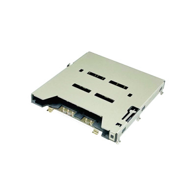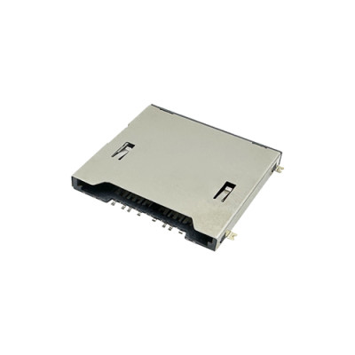
SIM Card Pinout Explained: C1–C8 Pin Functions, Wiring, and Interface Design
SIM Card Pinout Explained: C1–C8 Pin Functions, Wiring, and Interface Design
Primary Keyword:SIM Card Pinout
Secondary Keywords:SIM card pinout C1 C8, SIM card connector pinout, SIM socket pinout, SIM card C1 C8, 6 pin SIM connector, 8 pin SIM connector, SIM interface, SIM card wiring, SIM card connector, Nano SIM pinout, Micro SIM pinout
Meta Title:SIM Card Pinout Explained: C1–C8, Wiring & Interface Design
Meta Description:Learn the SIM card pinout from an engineer’s perspective. Understand C1–C8 functions, SIM-to-module wiring, 6-pin vs. 8-pin sockets, card detection, and PCB design considerations.
SIM Card Pinout: A Practical Guide for Hardware Engineers
When designing a cellular device, knowing the SIM card pinout is only the first step.
A hardware engineer also needs to understand how the SIM card contacts connect to the SIM socket, how the socket maps to a cellular module, which contacts are actually required, and what needs to be considered during PCB layout.
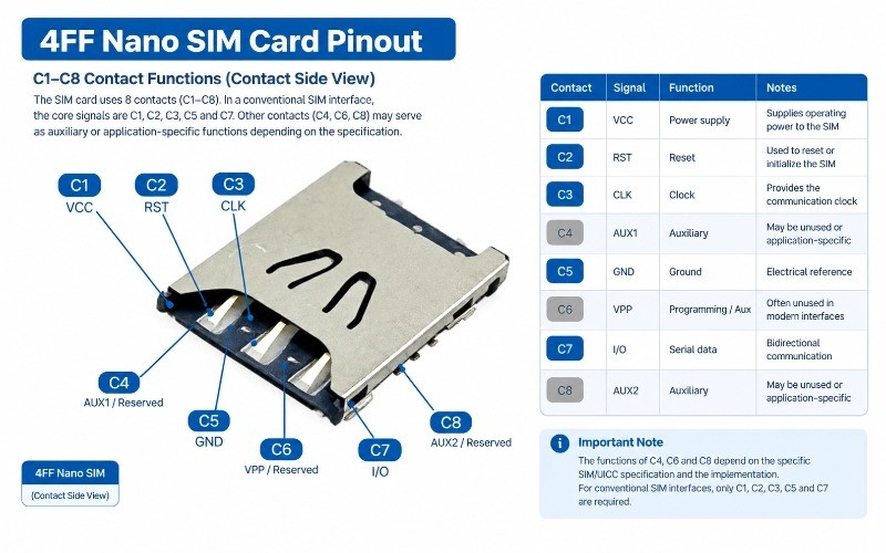
The standard SIM contact area is commonly identified as C1 through C8. The five fundamental signals used by a conventional SIM interface are typically:
C1 — VCC
C2 — RST
C3 — CLK
C5 — GND
C7 — I/O
Other contacts, such as C4, C6, and C8, can have reserved or application-specific functions depending on the relevant specification and implementation.
For engineers, the important point is this:
SIM card contact numbering, SIM socket pin numbering, and cellular module pin numbering are not necessarily the same thing.
This guide explains the SIM card pinout from an engineering and hardware-design perspective, including C1–C8 functions, socket selection, SIM wiring, PCB considerations, and troubleshooting.
1. What Is a SIM Card Pinout?
A SIM card pinout describes the physical contact positions and corresponding electrical functions on a SIM card.
The SIM card is not simply a storage component. It provides a standardized electrical interface through which a cellular modem or host device communicates with the card.
The contact area is conventionally identified using labels such as C1, C2, C3, and so on.
From a hardware design perspective, the signal path normally looks like this:
SIM Card → SIM Socket → PCB Traces → Cellular Module
Each stage introduces different design considerations.
For example, the SIM card has standardized contact positions, while the connector manufacturer defines how those contacts appear on the socket terminals. The cellular module manufacturer then defines the corresponding module-side signals.
Therefore, engineers should always check three documents during a hardware design:
The applicable SIM/UICC specification
The SIM connector or socket datasheet
The cellular module hardware design guide
Do not assume that connector Pin 1 automatically means SIM contact C1.
2. SIM Card Pinout: C1–C8 Pin Functions
The following table provides a practical overview of the standard SIM contact assignment.
| SIM Contact | Typical Signal | Function | Engineering Note |
| C1 | VCC | Power supply | Supplies operating power to the SIM |
| C2 | RST | Reset | Used to reset or initialize the SIM |
| C3 | CLK | Clock | Provides the communication clock |
C4 | AUX1 | Auxiliary / application-specific | May be unused or assigned in later profiles |
C5 | GND | Ground | Electrical reference |
C6 | VPP / auxiliary | Programming / application-specific | Often unused in modern basic interfaces |
C7 | I/O | Serial data | Bidirectional communication with the SIM |
C8 | AUX2 | Auxiliary / application-specific | May be unused or assigned in later profiles |
C1 — VCC
C1 is the SIM power supply contact.
The required operating voltage depends on the SIM interface implementation and the supported voltage class.
When designing a SIM interface, engineers should not simply assume a fixed voltage. The cellular module's hardware design guide should be checked to determine the supported SIM voltage and activation behavior.
C2 — RST
C2 is the reset signal.
The host or cellular module uses the reset line as part of SIM initialization and communication procedures.
An incorrect RST connection can prevent the module from successfully initializing the SIM even when VCC is present.
C3 — CLK
C3 provides the clock signal required for communication.
CLK is one of the signals that deserves particular attention during PCB layout. Excessive trace length, poor routing, coupling, or inappropriate protection components can affect signal quality.
C4 — AUX1
C4 is a contact that may be reserved in a basic SIM interface but can have an application-specific function in later profiles or implementations.
Do not connect C4 based solely on a generic pinout diagram. Follow the relevant module and SIM interface documentation.
C5 — GND
C5 is the ground contact.
A reliable ground connection is essential for both power integrity and signal integrity.
The SIM socket and PCB ground design should be considered together rather than treating the ground contact as an afterthought.
C6 — VPP / Auxiliary Function
C6 is associated with VPP in the base contact assignment and can have application-specific use in later implementations.
For many modern cellular module designs, C6 is not required for the basic SIM communication path.
Always verify the module's hardware design guide before leaving this contact unconnected or assigning it another function.
C7 — I/O
C7 is the bidirectional serial data interface.
It carries communication between the SIM and the cellular module.
Because I/O is an active signal, correct routing, grounding, protection, and connector contact quality are important for reliable operation.
C8 — AUX2
C8 is another auxiliary contact.
Like C4, its function depends on the relevant specification and implementation.
For a conventional SIM interface, it may remain unused. Do not assume that every eight-contact SIM socket requires every contact to be electrically connected.
3. Which SIM Card Pins Are Actually Required?
For a conventional SIM interface, the essential electrical path normally consists of:
VCC + RST + CLK + GND + I/O
In terms of SIM contacts:
C1 + C2 + C3 + C5 + C7
This explains why SIM connectors with fewer electrical contacts can still support conventional SIM communication.
However, the number of terminals visible on a connector drawing should not automatically be interpreted as the number of SIM electrical contacts.
A connector may also include:
Card-detect contacts
Mechanical switch contacts
Shield or cover grounding
Other auxiliary terminals
This distinction is important when selecting a connector for a new PCB.
4. SIM Card Pinout vs. SIM Socket Pinout
One of the most common mistakes in hardware design is treating the SIM card pinout and SIM socket pinout as the same thing.
They are related, but they are not necessarily identical.
SIM card pinout
The SIM card defines contact positions such as:
C1, C2, C3, C4, C5, C6, C7, C8
SIM socket pinout
The connector manufacturer defines PCB-side terminals according to the mechanical and electrical construction of that particular socket.
For example, a socket datasheet may identify terminals as:
Pin 1, Pin 2, Pin 3, Pin 4...
Those terminal numbers need to be mapped to the corresponding SIM contacts.
Cellular module pinout
The modem may use signal names such as:
SIM_VCC
SIM_RST
SIM_CLK
SIM_IO
SIM_DET
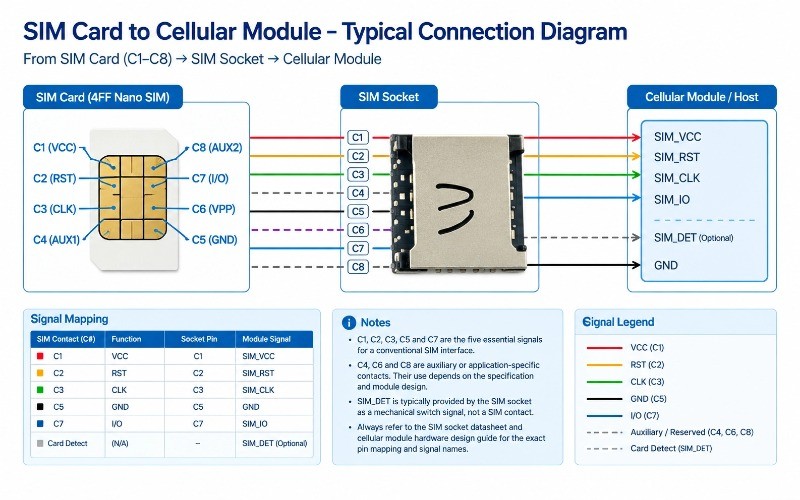
The actual PCB design therefore requires a mapping between all three:
SIM Contact → Socket Terminal → Module Signal
This is why engineers should always use the connector's actual datasheet and the module's hardware design guide before releasing a PCB.
5. SIM Card Wiring: From C1–C8 to a Cellular Module
A simplified conventional connection can be represented as:
SIM SOCKET
│
SIM C1 ──────────────┤── SIM_VCC
SIM C2 ──────────────┤── SIM_RST
SIM C3 ──────────────┤── SIM_CLK
SIM C5 ──────────────┤── GND
SIM C7 ──────────────┤── SIM_IO
│
▼
CELLULAR MODULE
If the connector includes a card-detect switch, that signal may be routed separately:
SIM SOCKET
│
├── C1 → SIM_VCC
├── C2 → SIM_RST
├── C3 → SIM_CLK
├── C5 → GND
├── C7 → SIM_IO
│
└── CARD DETECT → SIM_DET / GPIO
The exact signal names and recommended external components vary by module manufacturer.
6. 6-Pin vs. 8-Pin SIM Connectors
When engineers search for a SIM card connector pinout, they often encounter 6-pin, 7-position, 8-pin, or other connector configurations.
The key is to distinguish:
SIM contacts
from
connector terminals and switches.
A conventional SIM interface only needs the five core signals:
VCC
RST
CLK
GND
I/O
A connector may provide additional terminals for:
Card detection
Auxiliary contacts
Shield grounding
Other mechanical functions
Therefore, connector selection should be based on the actual electrical and mechanical requirements rather than pin count alone.
Questions to ask before selecting a SIM connector
Which SIM form factor is required?
Is card detection required?
What PCB height is available?
How often will the card be inserted and removed?
Is push-push, push-pull, or hinged operation preferred?
What environmental conditions will the device experience?
Are there special retention requirements?
What are the required contact and plating specifications?
Does the connector footprint match the intended PCB layout?
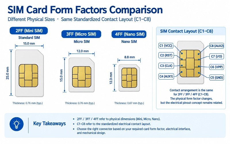
7. SIM Form Factors: 2FF, 3FF, and 4FF
SIM card form factor and SIM electrical pinout are related but different concepts.
Common physical formats include:
| Form Factor | Common Name | Approx. Size |
| 2FF | Mini SIM / Standard SIM | 25 × 15 mm |
| 3FF | Micro SIM | 15 × 12 mm |
| 4FF | Nano SIM | 12.3 × 8.8 mm |
The electrical contact arrangement is based on standardized SIM/UICC interfaces, while the physical dimensions change as devices become smaller.
This means an engineer selecting a connector should first determine the required card form factor, then select a compatible connector design.
A Nano SIM connector cannot simply be substituted for a Micro SIM connector because the electrical concept is similar. Mechanical dimensions, contact geometry, card thickness, retention, and PCB footprint must all match.
8. 1.8 V, 3 V, and SIM Interface Voltage Considerations
Voltage compatibility is another important part of SIM interface design.
SIM specifications have historically supported different voltage classes, and modern cellular modules commonly support lower-voltage operation.
From an engineering perspective, the important rule is:
Do not select the SIM connector based only on the SIM card's nominal voltage. Check the complete module interface specification.
The connector itself is primarily a mechanical and electrical contact component. The cellular module and SIM interface circuitry determine how the card is powered and communicated with.
When designing the interface, check:
1.Supported SIM voltage
2.Module SIM interface specification
3.Power-up sequence
3.Signal voltage levels
4.ESD protection requirements
5.Connector contact resistance
6.PCB routing requirements
A connector manufacturer should also provide the relevant electrical and mechanical specifications for the selected component.
9. SIM Card Connector PCB Design Considerations
The SIM socket may be a small component, but its PCB implementation can affect system reliability.
9.1 Keep Critical Signal Paths Controlled
The CLK and I/O signals are part of the communication interface.
Avoid unnecessarily long traces and excessive routing complexity.
9.2 Pay Attention to Grounding
C5 provides the SIM ground reference.
The connector footprint and surrounding PCB ground structure should provide a reliable electrical return path.
9.3 Consider ESD Protection
SIM cards are user-accessible components in many products.
A removable card can expose the interface to electrostatic discharge during insertion and removal.
The protection strategy should be designed together with the cellular module manufacturer's recommendations.
9.4 Verify Connector Orientation
Before PCB release, verify:
Card insertion direction
Contact-side orientation
Pin 1 location
Connector footprint orientation
Top/bottom mounting
Card-detect switch position
A mirrored connector footprint can create a complete electrical failure even when the schematic looks correct.
9.5 Review the Mechanical Stack-Up
The connector must match:
SIM card thickness
PCB thickness
Enclosure clearance
Insertion direction
Ejection mechanism
Retention requirements
This becomes particularly important with low-profile Nano SIM connectors.
10. Card Detection: SIM_DET Is Not the Same as C1–C8
Many engineers initially assume that a SIM card's card-detect signal is another C-contact.
In many connector designs, card detection is implemented using a mechanical switch inside the connector.
The switch can report whether a card has been inserted to the host processor or cellular module.
A simplified system looks like:
SIM CARD
│
▼
SIM SOCKET
│
├── C1 → VCC
├── C2 → RST
├── C3 → CLK
├── C5 → GND
├── C7 → I/O
│
└── Card Detect Switch → SIM_DET
│
▼
MCU
This distinction is especially important when selecting a connector.
If firmware needs to distinguish between:
No SIM inserted
SIM inserted
SIM rejected
the hardware may need an appropriate card-detect implementation.
Therefore, card detection should be considered before the PCB footprint is finalized.
11. How to Choose a SIM Card Connector
A technically correct SIM card pinout is only part of the connector selection process.
For a new product, evaluate the following:
Electrical Requirements
Required SIM contacts
Contact resistance
Voltage compatibility
Signal integrity
ESD requirements
Grounding
Mechanical Requirements
2FF, 3FF, or 4FF
Connector height
PCB footprint
Insertion direction
Retention method
Card thickness
Available enclosure space
User Interaction
Push-push
Push-pull
Hinged
Card detect
Ease of replacement
Reliability
For industrial, automotive, IoT, or field-service applications, also consider:
Vibration
Shock
Temperature
Corrosion resistance
Mating-cycle requirements
Contact stability
12. Moarconn SIM Card Connector Solutions
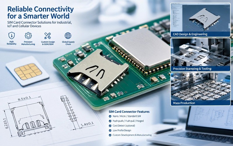
For engineers working on a new SIM-enabled product, understanding the pinout is only the beginning. The next step is selecting a connector that fits the electrical, mechanical, and manufacturing requirements of the product.
Moarconn specializes in card connector development and manufacturing, including SIM card connectors, SD card connectors, Micro SD connectors, and smart card connectors.
Its SIM connector solutions cover different SIM form factors and mechanical configurations, including Nano SIM, Micro SIM, and standard SIM, with options such as push-push, push-pull, and hinged structures.
Depending on the product series, connector options can also include card-detection functionality and different low-profile configurations.
For OEM and ODM projects, Moarconn provides a development process covering requirements confirmation, quotation, product design, tooling, sample production, trial production, and mass production.
This makes the connector selection process more than simply choosing a component from a catalog.
When a Standard SIM Connector Is Not Enough
A custom connector may be appropriate when the product has requirements such as:
Limited PCB height
Unusual enclosure geometry
Specific insertion direction
Custom card-detect requirements
Special retention requirements
High insertion-cycle requirements
Industrial or automotive environmental requirements
Existing PCB footprint constraints
OEM/ODM mechanical integration
Why Work With a Connector Manufacturer Early?
The SIM socket affects more than the electrical schematic.
It also affects:
PCB footprint
Product height
Enclosure design
Card insertion mechanism
Mechanical retention
Assembly process
Supply-chain planning
For that reason, involving the connector manufacturer early can help identify mechanical or manufacturing constraints before tooling and PCB layout are finalized.
MoarConn supports connector development from initial requirements through product design, samples, trial production, and mass production.
13. SIM Card Pinout Troubleshooting Checklist
If a cellular module reports “SIM not detected”, use a systematic hardware check instead of replacing the SIM card immediately.
Step 1: Check VCC
Measure the SIM supply at the connector.
Confirm that:
The voltage is within the module specification.
The supply appears during SIM initialization.
There is no short to ground.
Step 2: Check GND
Verify continuity between:
SIM C5 → PCB GND → Cellular Module GND
Step 3: Check RST
Confirm that the reset signal reaches the correct SIM contact.
Step 4: Check CLK
Use an oscilloscope or appropriate measurement equipment to verify that the expected clock activity is present during initialization.
Step 5: Check I/O
Check the C7/I/O connection between the SIM and cellular module.
A missing or incorrectly mapped I/O line can prevent successful SIM communication.
Step 6: Check Card Detection
If the connector has a card-detect switch:
Verify switch operation.
Check SIM_DET logic level.
Confirm the firmware configuration.
Step 7: Inspect the Connector
Look for:
Bent contacts
Contamination
Poor solder joints
Incorrect footprint
Mechanical damage
Incorrect connector orientation
Insufficient contact force
Step 8: Verify the Datasheets
Finally, compare the actual PCB against:
1.SIM specification
2.Connector datasheet
3.Cellular module hardware design guide
This three-document check can often reveal mapping errors faster than debugging the firmware.
14. Common SIM Card Pinout Design Mistakes
Mistake 1: Assuming Connector Pin 1 = SIM C1
Always verify the connector's contact mapping.
Mistake 2: Treating All C1–C8 Contacts as Required
A conventional interface generally uses the five core contacts:
C1, C2, C3, C5, C7
Other contacts may be unused or application-specific.
Mistake 3: Ignoring Card Detect
If the system needs mechanical SIM presence detection, choose a connector with an appropriate detection switch.
Mistake 4: Choosing the Connector by Size Only
A connector that fits a Nano SIM mechanically may still have the wrong height, footprint, retention mechanism, or detection configuration.
Mistake 5: Copying a Generic Pinout Into a New Design
Generic diagrams are useful for understanding the interface, but the final design should always follow the actual connector and module documentation.
15. SIM Card Pinout Design Checklist for Engineers
Before releasing a SIM-enabled PCB, verify the following:
Electrical
C1/VCC is correctly mapped
C2/RST is correctly mapped
C3/CLK is correctly mapped
C5/GND is correctly mapped
C7/I/O is correctly mapped
Voltage compatibility is verified
ESD protection has been reviewed
Unused contacts are handled according to the relevant design documentation
Connector
Correct SIM form factor
Correct connector orientation
Correct PCB footprint
Correct connector height
Card-detect requirement confirmed
Retention mechanism selected
Required mating-cycle performance confirmed
PCB
CLK routing reviewed
I/O routing reviewed
Ground path reviewed
ESD path reviewed
Enclosure clearance checked
SIM insertion/removal path verified
Manufacturing
SMT process compatibility checked
Connector placement verified
Solder-joint inspection considered
Mechanical tolerance reviewed
Sample validation completed before mass production
16. FAQ: SIM Card Pinout
What are the 8 pins on a SIM card?
The SIM contact area is commonly identified as C1 through C8. Typical assignments include VCC, RST, CLK, GND, and I/O, while other contacts can have reserved or application-specific functions.
Which SIM pins are actually used?
A conventional SIM interface typically requires five core contacts:
C1, C2, C3, C5, and C7.
The exact implementation should be verified against the cellular module and SIM interface specifications.
What is C1 on a SIM card?
C1 is typically the VCC power contact.
What is C2 on a SIM card?
C2 is the reset contact.
What is C3 on a SIM card?
C3 is the clock contact.
What is C5 on a SIM card?
C5 is the ground contact.
What is C7 on a SIM card?
C7 is the bidirectional I/O data contact.
Are SIM card pinouts the same for Nano, Micro, and Mini SIM?
The physical form factors are different, but the underlying SIM contact assignment is standardized. The connector must still be selected to match the specific card form factor and mechanical dimensions.
Is SIM socket pin numbering the same as SIM card C1–C8?
Not necessarily. SIM card contacts use the C1–C8 terminology, while a connector manufacturer may use its own terminal numbering. Always check the connector drawing.
Do I need an 8-pin SIM connector?
Not necessarily. A conventional SIM interface can operate using the five core contacts. Whether a 6-position, 7-position, 8-position, or other connector configuration is appropriate depends on the required electrical and mechanical features.
What should I do if my modem cannot detect the SIM?
Start by checking:
VCC → GND → RST → CLK → I/O → Card Detect → Connector → PCB Layout
Then compare the implementation against the cellular module's hardware design documentation.
17. Final Engineering Takeaway
Understanding the SIM Card Pinout is not simply a matter of memorizing:
C1 = VCC
C2 = RST
C3 = CLK
C5 = GND
C7 = I/O
For a reliable product, engineers need to understand the complete interface:
SIM Contact → SIM Connector → PCB → Cellular Module
The connector must match the SIM form factor, electrical interface, mechanical constraints, card-detection requirements, and product environment.
For compact IoT products, automotive telematics, industrial equipment, routers, communication devices, and other cellular products, the SIM connector is a small component with a direct impact on both electrical connectivity and mechanical reliability.
Moarconn provides SIM card connector solutions for different form factors and mechanical requirements, together with connector development and OEM/ODM manufacturing support.
If you already have a PCB drawing, SIM form factor, required connector height, or card-detect requirement, these specifications can be used as the starting point for selecting or developing a suitable SIM card connector.
References for Further Engineering Research
ISO/IEC 7816 contact-position framework
ETSI TS 102 221 for UICC/SIM-related form factors and specifications
Cellular module hardware design documentation
Individual SIM connector manufacturer's datasheet and recommended PCB footprint
For any production design, always use the latest applicable specification and the exact datasheet for the selected cellular module and SIM connector.